Researchers create nanostructures of previously impossible materials for optoelectronics
In technology, it is a rather frequent task to change the physical properties of a material by adding certain amounts of additional elements. In crystals, however, the incorporation of foreign materials into the lattice structures often hits physical limits. A new method has now been developed at the Vienna University of Technology to achieve previously unattainable mixing ratios between germanium and desired foreign atoms. This results in new materials with significantly altered properties.
“The targeted incorporation of foreign atoms into a crystal in order to improve its properties is actually a standard method,” says Sven Barth from the Institute of Material Chemistry at TU Vienna. Modern electronics is based on semiconductors with certain additives – for example, silicon crystals in which foreign atoms such as phosphorus or boron are incorporated.
Germanium, a material used in many semiconductors, should also fundamentally change its properties and behave more like a metal if you add a sufficient amount of tin – this was already known in theory. In practice, however, this has not yet been possible.
From a naive point of view, one could simply try to heat up the two elements, mix them well in liquid form and then solidify them, as has been done for thousands of years in order to produce metal alloys. However, in this case, this simple thermodynamic method fails because the added atoms do not fit efficiently into the lattice system of the crystal. The higher the temperature, the more mobile are the atoms in the material. This can lead to the point that these foreign atoms exit the crystal after a successful incorporation and only a very small concentration of these atoms remains to be found inside.
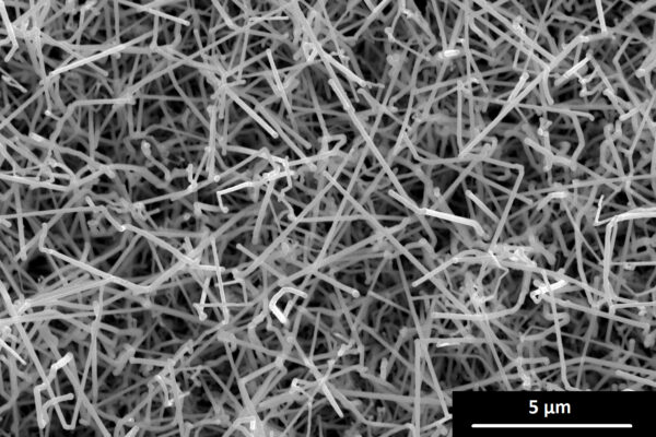
Barth’s team therefore developed a new approach that combines particularly fast crystal growth with very low process temperatures. During the formation of the crystal, the correct amount of foreign atoms is continuously incorporated. The crystals grow in the form of small wires or rods in nano-size form at much lower temperatures than before, i. e. about140-230°C. “As a result, the built-in atoms are less mobile from the outset, the diffusion processes are slow, and most atoms remain where they are needed,” explains Barth.
With this method, it has been possible incorporate up to 28% tin and 3.5% gallium into germanium. This is considerably more than was previously possible thanks to the usual thermodynamic combination of these materials – namely 30 to 50 times.
For microelectronics, this opens up new horizons: “Germanium can easily be combined with existing silicon technology on the one hand, and the addition of tin or gallium in such high concentrations offers highly interesting opto-electronic applications on the other,” says Barth. Since the physical properties of germanium are significantly changed by these additives, the novel materials could be used for infrared lasers, photodetectors or innovative LEDs in the infrared range, the researcher believes.
Original publication: https://pubs.acs.org/doi/pdf/10.1021/acsnano.7b07248
 If you enjoyed this article, you will like the following ones: don't miss them by subscribing to :